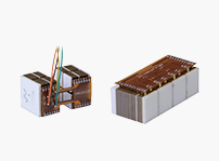
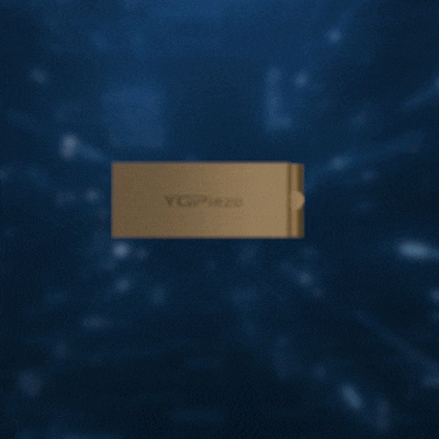
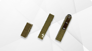
Material | Device
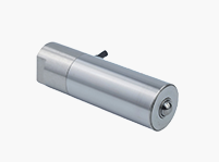
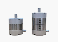
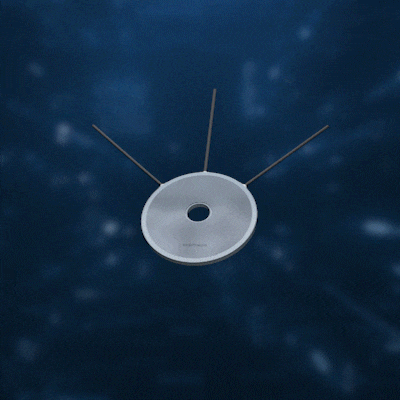
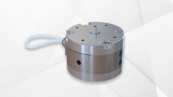
Actuator | Motor
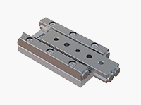
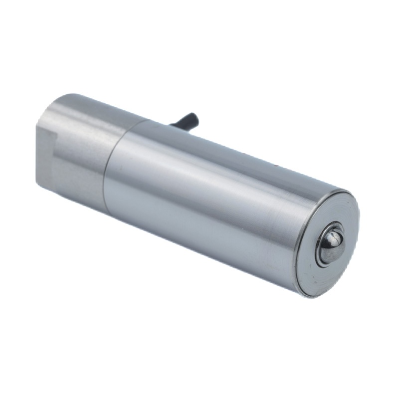
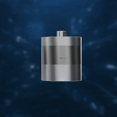
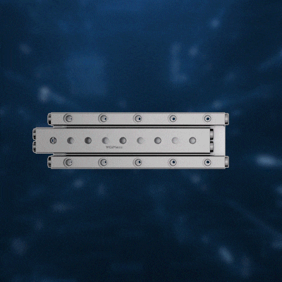
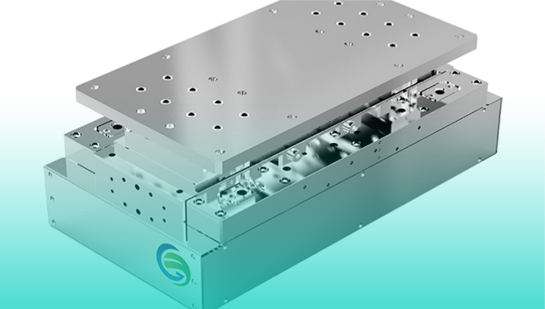
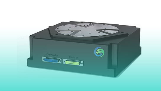
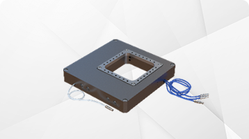
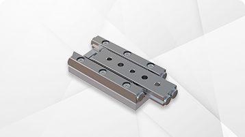
Positioning Stage | System


The Curie brothers discovered the piezo effect.
The piezo effect of BaTiO3 was discovered.
Lead zirconate titanate (PZT) was discovered and became the most widely used piezoceramic material.
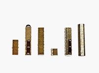
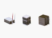
laminated ceramics have been widely applied.

When certain materials are subjected to pressure or tension along specific directions, electric charges appear on two opposite surfaces as deformation occurs; when the external force is removed and the deformation disappears, the material returns to an uncharged state.
Conversely, applying an electric field in the polarization direction (on the two surfaces where charges are generated) causes mechanical deformation.These two phenomena are like how engines and motors achieve mutual conversion between electrical and mechanical energy.
These two phenomena are like how engines and motors achieve mutual conversion between electrical and mechanical energy.


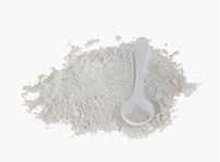
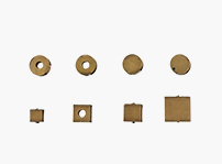
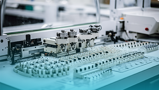
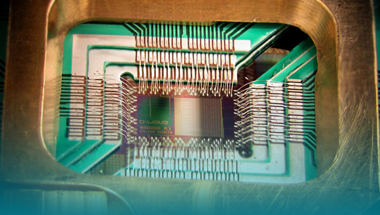
From powder materials to complex positioning products, YiNGUAN has the entire in-house production capacity.

By aligning with client needs, YiNGUAN has developed comprehensive technology platforms encompassing R&D, testing, and quality assurance.

YiNGUAN partners with Domestic and international institutions for cutting-edge R&D in piezo materials and applications.

Flexible Engineering Design and Short Delivery Cycle.Can flexibly adjust the plan and process according to actual circumstances; Short delivery cycle.

A team with extensive engineering experience has achieved comprehensive self-developed capabilities in the design and manufacturing of piezo products.

Comprehensive Technical Support and Service Network. There are eight service centers in China.