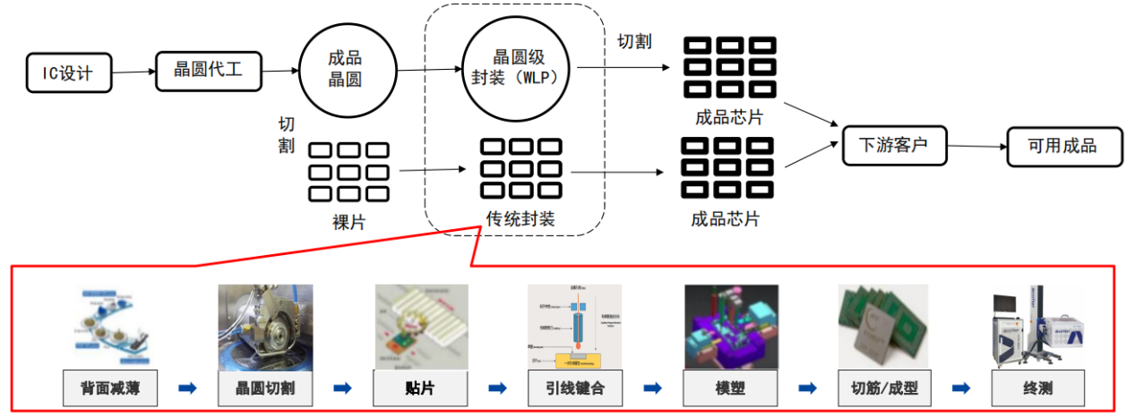
In the first half of 2024, the global semiconductor industry shows signs of recovery. With the rapid development of AI and HPC, the requirements for chip performance and power consumption are continuously increasing. Chiplet and 2.5D/3D technologies are driving the adoption of advanced techniques such as HBM, making them the primary direction for future development. Thinning equipment is a key core device for chip stacking technology and advanced packaging technology, and it will have extensive applications in the future.

(Sources: Zhongwei Consulting, 3M, Befor Capital, Huajin Securities Research Institute)
The wafer thinning machine is a key equipment that utilizes tribology principles to achieve the wafer thinning process in order to meet the requirements of packaging processes. The function of wafer thinning process is to grind the backside substrate material of the completed wafer (mainly silicon wafers), removing a certain thickness of material, in order to meet the requirements of subsequent packaging processes as well as the physical strength, thermal performance, and size requirements of the chip. According to information from the Electronics Engineering Magazine and AIBON Semiconductor Network, the thicknesses of 6-inch, 8-inch, and 12-inch wafers are 625, 725, and 775μm respectively. Over 90% of the total thickness of the wafer is to ensure that the wafer has sufficient strength in manufacturing, testing and transportation.
With the increasing application of 3D packaging, the wafer thickness is required to be reduced to 50-100 μm or even below 50 μm to achieve better heat dissipation effect and high-density packaging. This will significantly increase the quality requirements for thinning equipment.
The global thinning machine market is highly concentrated, and domestic substitution is on the way. According to YH Research, China's thinning machine market accounts for about 51% of the global market share, which is one of the most important consumer markets in the world, and the growth rate is higher than that of the world. However, the thinning machine has high complexity, technical difficulty and high market access threshold, and has been highly monopolized by foreign manufacturers for a long time. The main manufacturers of thinning machines in the global market include Japan DISCO, Japan TOKYO SEIMITSU, Japan KOYO SEIKO, Germany G&N and so on. According to public data, the global top three manufacturers occupy 85% of the market share. Among them, Japan DISCO and TOKYO SEIMITSU enjoy a high reputation in the industry for their excellent product performance and satisfactory service. In 2022, the total market share of the two enterprises has exceeded 65%, with a high market concentration.

(In the thinning process, tribological principles such as grinding and polishing are adopted.)
Wafer thinning methods include mechanical grinding, CMP, wet etching, as well as ADP and DCE. The two most common wafer thinning methods are traditional grinding/lapping and CMP. Lapping is currently the most traditional mechanical process for wafer backside thinning. The basic principle is that the backside of the wafer is ground by a rotating diamond grinding wheel. The substrates of diamond grinding wheels are usually ceramic and epoxy resin. CMP uses abrasive chemical slurry and a polishing pad for material removal. It can flatten the wafer and smooth the irregular topography on the surface, thus providing a better planarization effect than mechanical grinding.
The integrated thinning and polishing equipment has broad prospects. TSV requires wafers to be thinned to 50μm or even thinner to expose the copper at the bottom of the silicon vias and prepare for the next step of interconnection. However, at a thickness of less than 50μm, wafers can hardly tolerate the damage and internal stress to the wafer caused by grinding during the thinning process. Its rigidity also makes it difficult for the wafer to maintain its original flat state. At the same time, wafer transfer and handling in subsequent processes also encounter great problems. At present, the mainstream solution in the industry is to adopt the integrated machine concept, integrating wafer grinding, polishing, protective film removal, and dicing tape pasting and other processes in one equipment. The wafer is always adsorbed on the vacuum chuck from grinding until the dicing tape is pasted, and always remains in a flat state, thus solving the problem of transfer.
We can provide motion platform solutions compatible with 6/8/12-inch wafers, as well as multi-axis motion systems required for the integrated thinning and polishing equipment. In the motion system, X/Y axis bi-directional repeatability is up to ±0.5 μm, Z-axis bi-directional repeatability is up to ±0.2 μm, and T-axis bi-directional repeatability is up to ±2arcsec. Global flatness and straightness can reach micrometre level.
Our after-sales team covers all major cities in China to provide you with a full range of technical support.
(The latest industry and technical data comes from websites and other public information sources)