The wafer dicing equipment is a critical piece of equipment in the semiconductor back-end packaging and testing process, particularly for wafer dicing and WLP (wafer-level packaging) dicing. A single wafer usually comprises hundreds or even thousands of chips that are interconnected. The distance between the chips is 80μm to 150μm, known as the saw street. The process of separating each chip with independent electrical properties is called dicing saw. The semiconductor wafer dicing equipment divides wafers containing many chips into individual dies, preparing them for subsequent bonding processes. The quality and efficiency of dicing saw directly impact the quality of the chips and production costs.
The localization rate of wafer dicing equipment is relatively low and needs to be improved. According to the report, the global semiconductor dicing equipment market is estimated to be worth 12 billion annually, with China accounting for 25% of this market. Japan's DISCO dominates the entire semiconductor dicing equipment market, with domestic manufacturers holding less than 5% of the market share. However, with the embargo on Japanese semiconductor equipment, the market space and opportunities for domestic equipment are gradually opening up.
In a heterogeneous integration design, the manufacture of smaller chips necessitates more precise cutting, thereby increasing both the demand and precision requirements for wafer dicing equipment. According to statistics and forecasts by QYR the global wafer dicing equipment market reached $1.725 billion in 2023 and is expected to reach $2.516 billion by 2030, representing a CAGR of 5.4% from 2024 to 2030.
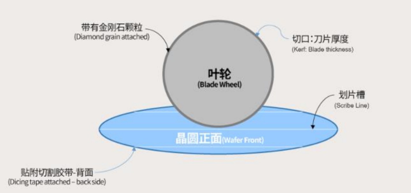
There are two main methods of wafer dicing: blade dicing and laser dicing. Blade dicing is the most widely used dicing technique, accounting for 80% of the market share. This method is typically employed for dicing thicker wafers (>100μm), offering high efficiency, low cost, and a long service life. Laser dicing, which accounts for approximately 20% of the market, is a non-contact processing method suitable for cutting thinner wafers (<100μm). It offers high precision and efficiency while avoiding damage to the silicon surface. For wafers thinner than 30μm, plasma dicing is used due to its fast cutting speed. The laser dicing saw is the most critical equipment for dicing chiplets in Chiplet technology.

(Blade Dicing Principle Diagram)
Given that the object of dicing is the expensive wafer, it is essential that the dicing equipment is both highly precise and reliable. Advanced 3D stacked packaging has led to a requirement for wafers and chips to become increasingly thin, with thicknesses even reaching below 50μm. Ultra-thin wafers are highly sensitive to mechanical stress and thermal stress, necessitating a dicing process that minimizes stress to the greatest extent possible.

For the field of semiconductor wafer dicing equipment, YINGUAN can provide high-speed and high-precision direct-drive motion systems based on years of experience in developing precision motion systems.
For linear axes, we can provide high-precision direct-drive solutions with bidirectional repeatability of ±0.5μm in XY axis and ±0.2μm in Z axis.
For rotary axes, we can provide high-precision, high-stiffness DD motors with bidirectional repeatability of ±2arcsec.
For wafer adsorption, we can provide porous ceramic suction cups compatible with a wide range of specifications.
At the same time, in order to reduce the risk of heat generation in the Z-axis, we can provide core part solutions such as magnetic levitation voice coil motor, water-cooling voice coil motor and magnetic springs. Through our highly modular design, it is easier for customers to achieve great configuration flexibility with low cost of ownership.
YINGUAN Semiconductor has an after-sales team covering all major cities in China to provide you with a full range of technical support.
(The latest industry and technical data comes from websites and other public information sources)