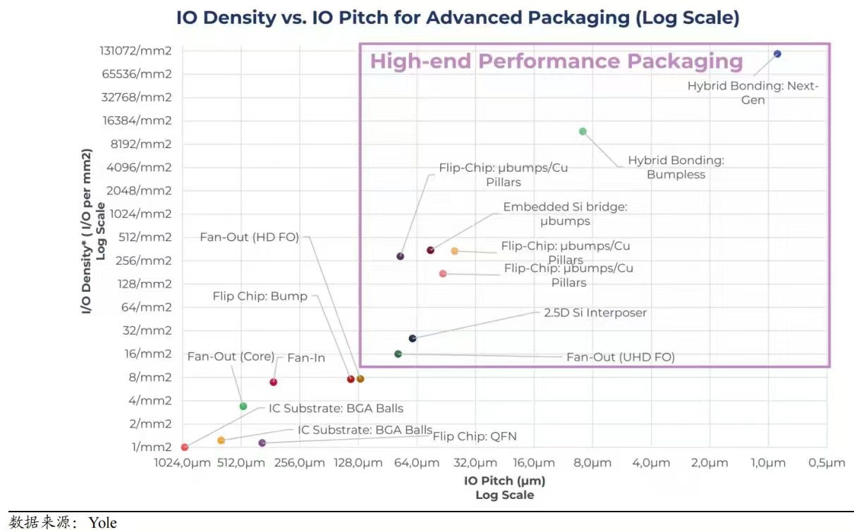
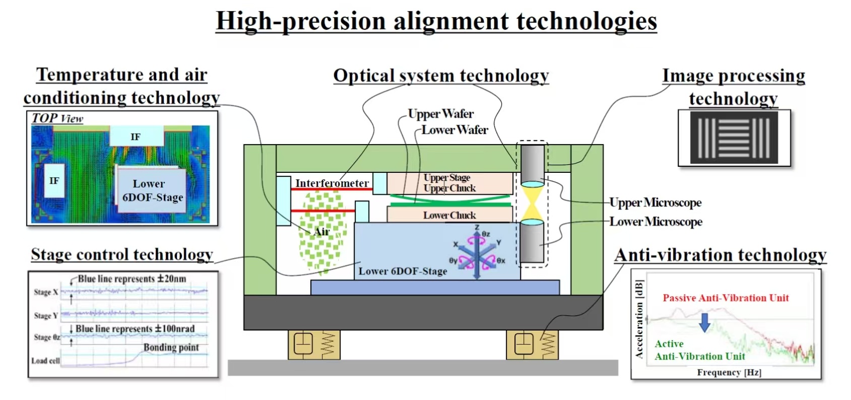
Hybrid bonding is the core path to achieve high-density stacking. With the improvement of vertical interconnection of multiple chips driven by high performance computing, the traditional micro-bump technology is faced with solder electromigration, thermal migration, bridge short-circuit and other reliability issues. It no longer meets the stacking requirements of extremely small stacking size and high I/O density, and the hybrid bonding (or Cu-Cu direct bonding) process arises at the historic moment. Flip-Chip bonding process pitch size is in 50~100μm, TCP (Tape Carrier Package) bonding process can reduce pitch size to 20 μm, and to further reduce the size, we must resort to hybrid bonding process. The essence of hybrid bonding is that Cu/SiO2 is polished to an extremely smooth surface, and with a little pressure or high temperature, permanent bonding can be achieved under the action of van der Waals forces. Since Cu-Cu, SiO2-SiO2 and Cu-SiO2 interfaces can be bonded simultaneously, it’s called hybrid bonding. The key points of this technology are the grinding method of low roughness, the high precision alignment method, the control method of wafer warpage and the control method of Cu soldering disc depression. In order to enhance surface bonding, processes such as plasma activation need to be added, followed by high-precision flip-Chip TCP to achieve hybrid bonding between multiple interfaces. Hybrid bonding has three core elements: high cleanliness (nm level control), high flatness and bond strength, and therefore it requires advanced front-end equipment and more expensive clean rooms. As you can see, hybrid bonding is more akin to a front-end process than a back-end packaging process.

Hybrid bonding process can be divided into two categories: Wafer to Wafer and Die to Wafer. The former is mainly applied to 3D NAND, CIS and other inter-Wafer stacking, which requires extremely high alignment accuracy and offset within 100 nm, and has already achieved mass production. A typical example is the 3D NAND X-stacking architecture of CXMT, where an independent manufacturing process is completed on the CMOS peripheral circuit and the NAND storage array, and then the two wafers are linked through hybrid bonding. Currently, EVG occupies about 82% of the W2W hybrid bonding market, followed by TEL. The value of EVG's single equipment is about 5-8 million euros per unit.
Die to Wafer is mainly applied to chip heterogeneous integration, such as SoIC, future HBM 4 stacking, etc., which requires consistent alignment accuracy and puts forward higher requirements for machine rate and cleanliness. Currently, D2W is not very mature, and BEIS has basically become a core player in this field with its excellent yield. TSMC's SoIC platform is based on this process, and AMD's MI300 series of AI chips released in 2023 involves TSMC's SoIC combined with CoWoS to achieve a chiplet stack of 12 dies. Apple's M5 series chips are also planned to use TSMC's SolC packaging technology. In order to meet customer demand, TSMC continues to expand production, with SoIC monthly production capacity of 2000 pieces by the end of 2023, the target of 6000 pieces/month by the end of 2024, and expected increase to 14,000 ~ 14,500 pieces/month in 2025. Currently, Besi equipment can achieve alignment accuracy of 0.5-0.1μm for connection point spacing below 10μm and connection density of 1w~100w connection points/mm2. The value volume of a single unit of equipment is also rapidly increasing. In the case of Besi, for example, the unit price of the same series of flip-Chip Die bonder is about US$500,000 per unit, while the unit price of the hybrid bonding equipment will be raised to US$1.5~2.5 million.
Currently, the hybrid bonding equipment is still in the product introduction period, and has initially realized industrialization in the field of image sensor, logic chip and memory field. Samsung will adopt hybrid bonding on both XCube and Saint platforms, respectively for memory - memory, logic chip - memory chip / logic chip stacking, while Intel will adopt it on Foveros, which is expected to take the lead in hybrid bonding technology between logic chips and interconnects in 2024. In addition, Hynix may also be the first to use hybrid bonding to its HBM4 chips. The core applications of hybrid bonding are: logic, SoIC 3D chiplet stacking, SRAM+Logic stacking and GAA backside power supply; memory, 3D NAND (W2W), HBM (>16 layers, D2W), 3D DRAM, etc.; and backside-illuminated CMOS image sensors. According to Yole forecast, although currently there is no HBM application of hybrid bonding, with the increasing number of stacked layers and higher integration requirements, the hybrid bonding process is expected to account for 36% of the process used for HBM in 2028. According to Besi, the demand for hybrid bonding systems is forecast to reach 1,400 units in 2030 under neutral assumptions, and the total market of the equipment will be 2.8 billion euros. According to Yole, the market for W2W and D2W hybrid bonding equipment is expected to reach $500 million / $230 million in 2027. Hybrid bonding has become the key layout direction of global semiconductor equipment factories. AMAT, ASMPT, Shibaura, TEL, SUSS, etc. and the domestic mainland companies including Tuojing Technology, Huazhuo Precision Technology have entered.

For the field of semiconductor hybrid bonding equipment, we can provide high-speed, high-precision Coarse-Fine Architecture motion systems based on years of experience in developing precision motion systems.
For rapid wafer placement, we can provide high-speed, high-precision air-bearing motion platforms, and for ultra-precision wafer alignment, we can provide piezoelectric positioning platforms with nm-level positioning accuracy.
For Z-axis, the core component solutions such as maglev voice coil motors, active water-cooled voice coil motor and magnetic spring can be customized, which can effectively improve the accuracy of Z-axis and reduce the risk of Z-axis heating. Through the highly modular design, it is easier for customers to achieve great configuration flexibility at a low cost.
Our after-sales team covers all major cities in China to provide you with a full range of technical support.
(The latest industry and technical data comes from websites and other public information sources)