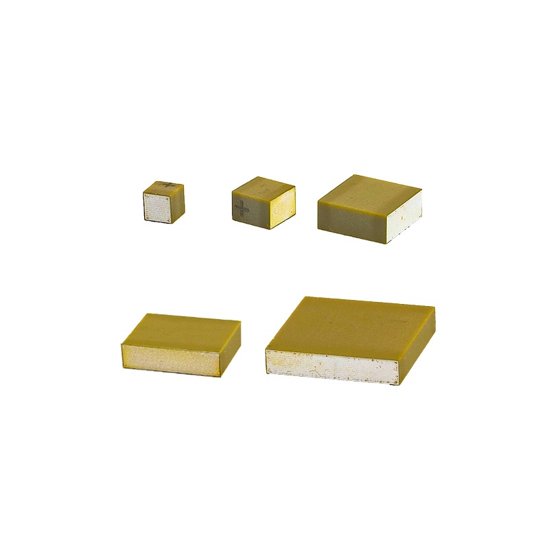
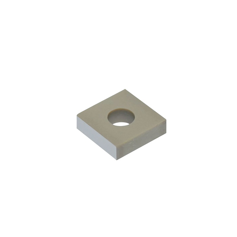
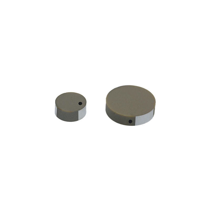
The Piezo Chip Actuator consists of multiple ceramic layers and electrode layers stacked and intersected internally, with external electrodes printed on both sides to lead out the internal electrodes. Through precision grinding processes, the height tolerance of each piezoelectric ceramic is controlled to be smaller than ±5μm. The company has achieved seamless integration from piezoelectric ceramic powder to the finished actuator, and mass production has been implemented. Currently, the products are applied in the fields of nanoscale positioning, precision manufacturing, and dispensing valve technology.
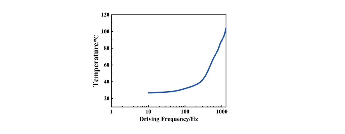
The figure above shows the temperature variation of the PAA-S7-2W device. It serves as a representative example, as the stack also exhibits similar patterns.
|
|
Dimensions |
Displacement* |
Blocking force** |
Electrical capacitance*** |
Resonant frequency |
|
Unit |
mm×mm×mm |
μm |
N |
nF |
kHz |
|
Tolerance |
|
±15% |
Max. value |
±15% |
±15% |
|
PAA-S2-2 |
2×2×2 |
2.5 |
160 |
22 |
565 |
|
PAA-S3-2 |
3×3×2 |
2.5 |
350 |
60 |
475 |
|
PAA-S5-2 |
5×5×2 |
2.5 |
1000 |
170 |
320 |
|
PAA-S7-2 |
7×7×2 |
2.5 |
1960 |
390 |
235 |
|
PAA-S7M-2 |
7×7×2 |
3 |
1960 |
610 |
235 |
|
PAA-S10-2 |
10×10×2 |
2.5 |
3900 |
800 |
165 |
*Displacement test: drive voltage range 0 to 150V, and PAA-S7M-2 drive voltage range 0~120V
**Blocking force test:The force that compresses the ceramic elongation to zero at a driving voltage of 150V
***Capacitance test conditions: ambient temperature environment, 1Vpp/1kHz
The tolerance of dimension AB within ±0.1mm, and the tolerance of dimension H within ±0.01mm
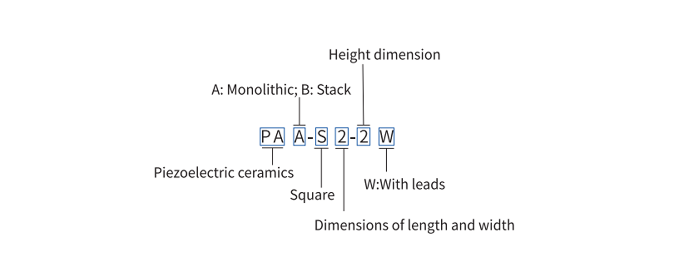
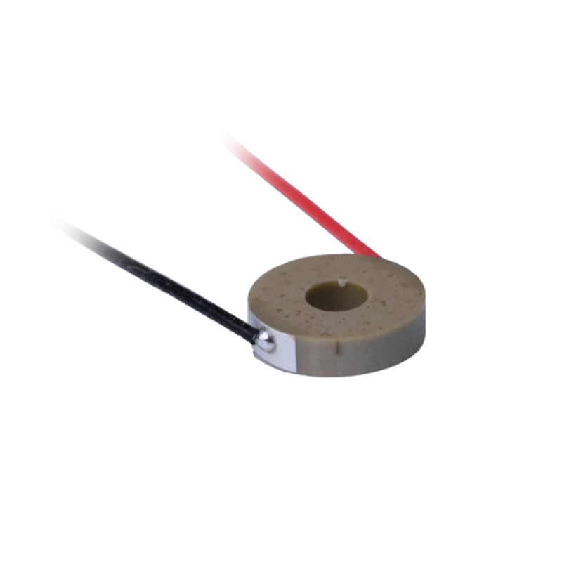
The default configuration does not involve soldering wire harness for the Piezo Chip Actuator
Optional soldering of standard wiring harness available, length 75mm, AWG32, PTFE insulation, followed by 'W' in the product code
Other specifications can be customized on request