Due to the various limitations of optical technology, electron beam imaging techniques have become indispensable as alternatives in advanced semiconductor processes.
E-Beam inspection, an application of scanning electron microscopy (SEM) technology, utilizes information generated by the interaction of high-energy electrons with the material on the wafer's surface for imaging. This is followed by image processing and analysis to detect wafer defects and critical dimensions.
EBI uses a focused electron beam as the detection source. During the EBI process, the incident electron beam stimulates the emission of secondary electrons. Defects or critical dimensions are detected through the collection and analysis of these secondary electrons. The main application is in the inspection of defects and critical dimensions in semiconductor components, with a primary focus on electrical defects and secondary focus on physical defects. Moreover, since the detection source is an electron beam, the results are not affected by certain surface physical properties like color anomalies, thickness variations, or defects from previous layers. Therefore, EBI can also be utilized to detect minute surface defects, such as gate etch residues.
E-beam inspection system consists of components including electron gun, electromagnetic lenses, condenser lenses, objective lens, steerer, detector, backend imaging system, as well as vacuum system and high-vacuum precision motion system. The system structure is illustrated in the following diagram:
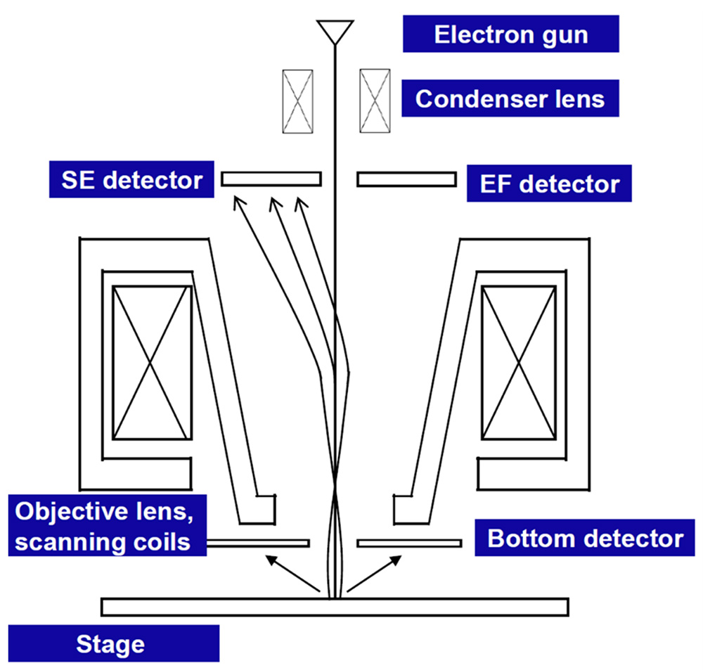
E-Beam Inspection Principles (Photo source: Internet)
The following key indicators are used to measure the performance of an E-Beam inspection system:
• Minimum spot size: This directly affects the minimum dimension of features that can be inspected.
• Acceleration voltage: Typically ranges from 10 to 100 KV. The higher acceleration voltages, the higher the resolution, making it easier to detect defects.
• Electron beam current: The greater the beam current, the faster the inspection speed. However, the maximum inspection speed is limited by the scanning frequency, and a larger beam current may also result in a larger beam spot size.
• Scanning speed: The faster the scanning speed, the quicker the inspection process becomes.
• Positioning accuracy of the vacuum motion system.
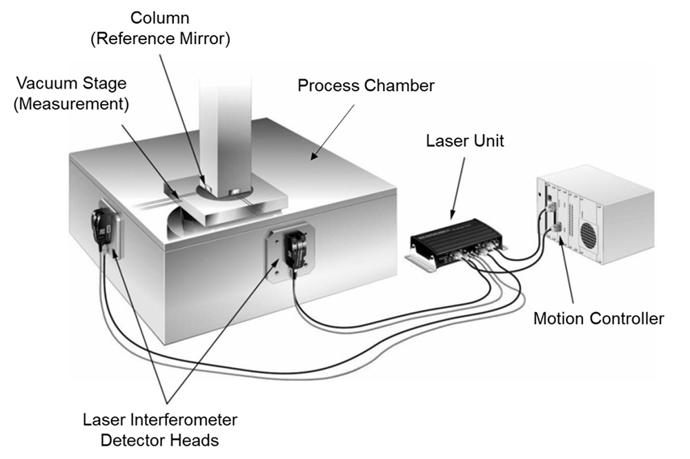
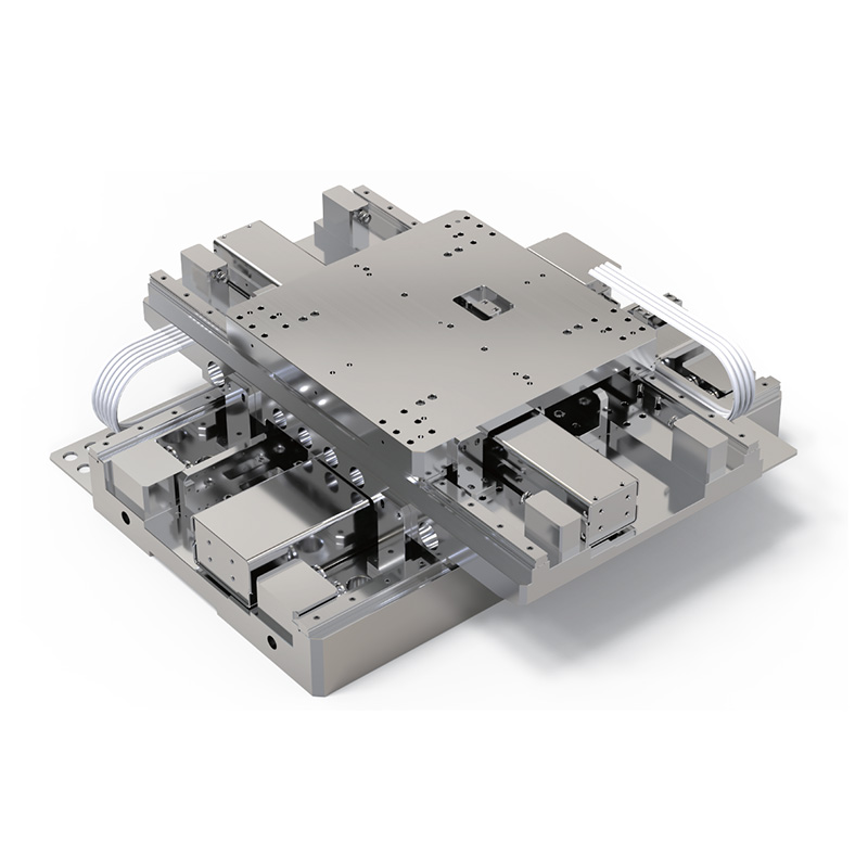
Schematic Diagram of the Vacuum Motion and Control System in E-beam wafer inspection system (Photo source: Internet)
Based on many years of experience in the development of vacuum products and high-end motion systems, YiNGUAN has developed the high-vacuum XY stage for E-Beam inspection system, which has achieved mass production and supplied to many domestic customers in batches. It is running stably in the domestic head Fab factory, with position stability up to ±2nm and speed uniformity <0.1% (speed is 100mm/s). It is also widely applied in CD-SEM, defects Review-SEM, etc. Electrostatic chuck has been mass-produced, supplied to many domestic customers, and are running stably in domestic head Fab factories.
In addition to supply high-precision vacuum motion system, YiNGUAN company also has been doing localization alternative of related key parts, include but are not limited to vacuum-compatible laser interferometers, vacuum-compatible piezoelectric motors, electrostatic chuck, vacuum-compatible cable, etc.