(Photo source: Internet)
The definition of overlay error is the plane distance between the centers of two layers of graphic structures. As the number of layers of integrated circuits continues to increase, lithography processes with multiple patterns and multiple exposures are widely used, and the overlay accuracy between circuit patterns formed in different steps becomes increasingly important. Misalignment caused by excessive overlay error will cause the entire circuit to fail and be scrapped. Overlay metrology system is used to ensure the correct alignment and placement of different levels of circuit graphics and the same layer of circuit graphics. Overlay metrology are typically performed after each lithography step.
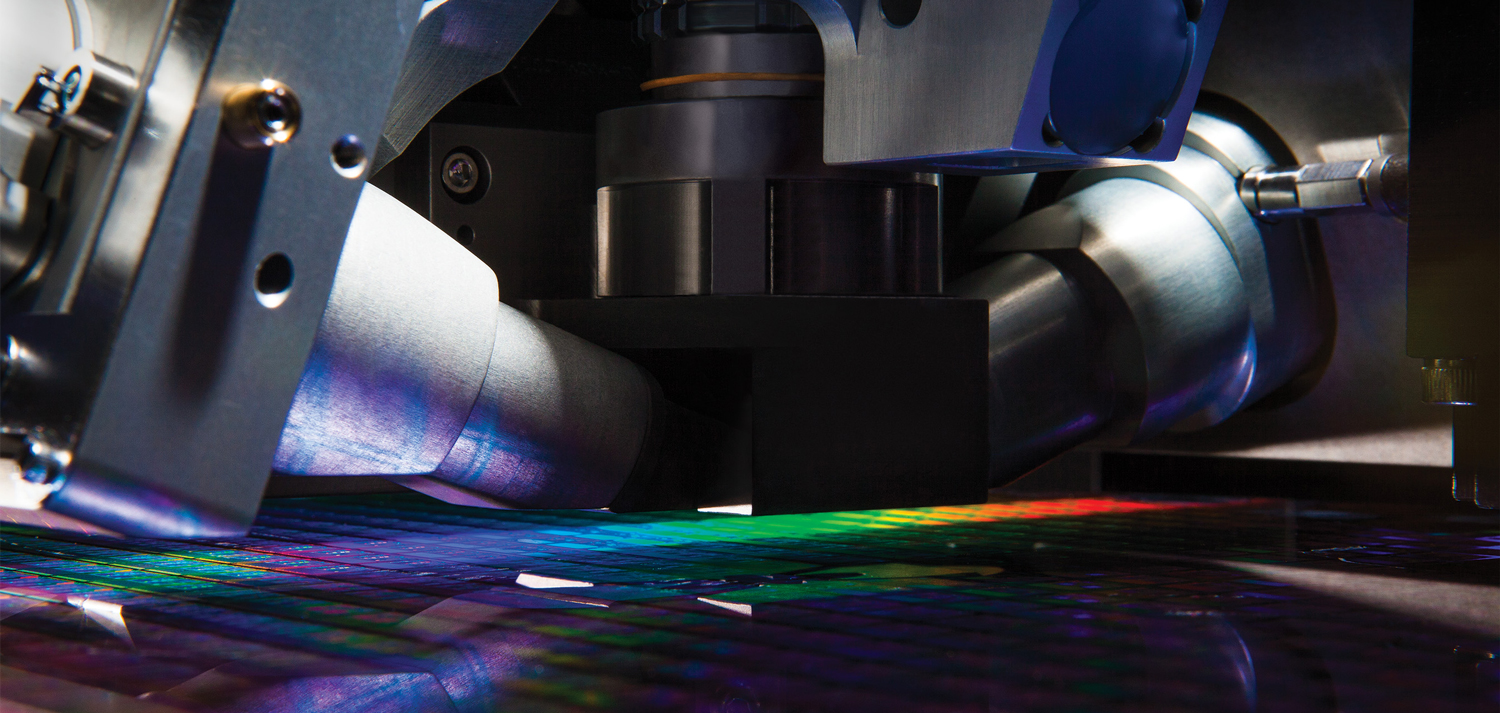
There are three methods for overlay metrology: optical microscopy (IBO), optical diffraction imaging (DBO), and scanning electron microscopy (SEM-OL). Optical microscopy imaging equipment is commonly used. The digital graphics of the two-layer overlay target graphics are obtained through the optical microscopy system, and then the boundary position of each layer of graphics is located through a software algorithm, and the center position is further calculated to obtain the overlay error; Optical diffraction device irradiates a beam of monochromatic parallel light onto gratings overlaying targets in different layers, and determines the error by measuring the uncertainty in the intensity of the diffracted beam. Scanning electron microscopes are mainly used for final overlay metrology after etching. The corresponding target pattern size is smaller, but the measurement speed is slower.
The international technology roadmap for semiconductor (ITRS) puts forward overlay error requirements for the lithography process of each technology node, as shown in Table 1. As can be seen from the table, as technology nodes advance, the allowable alignment deviation (i.e., overlay error) of key lithography layers shrinks by approximately 80%. For example, the overlay error requirement (mean+3σ) for critical layers in the 20nm node is 8.0nm.
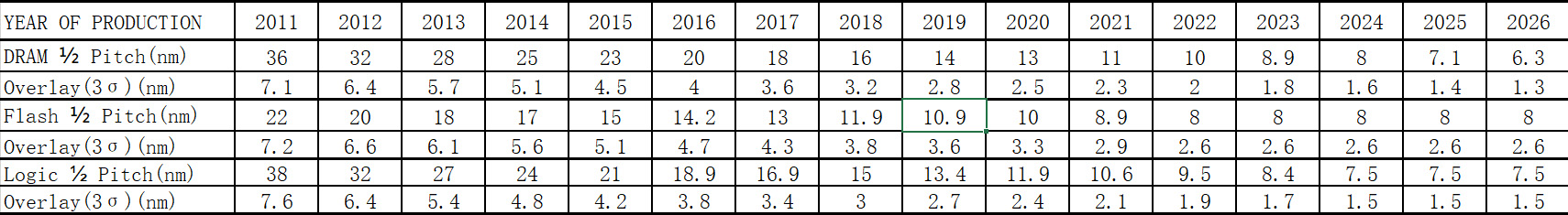
Table 1 Allowable overlay errors for each technology node (Photo source: Internet)
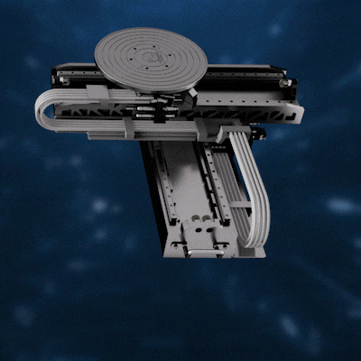
Based on its strong R&D capabilities, YiNGUAN Semiconductor can provide a high-end motion systems with a static jitter of 2nm and a maximum acceleration of 20m/s². In order to further improve the performance of the motion system and ensure its excellent motion setting performance, we can provide matching high-performance solutions with vibration isolation system. In addition, we can also customize vertical piezoelectric motion systems with static jitter up to 2nm. YiNGUAN Semiconductor has an after-sales team covering major cities across the country to provide you with a full range of technical support.