(Photo source: Internet)
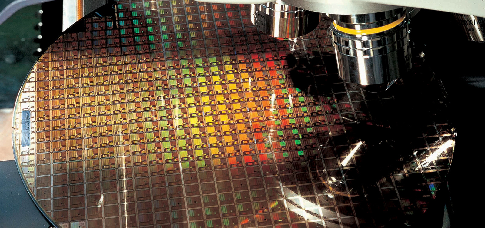
With the rapid development of the semiconductor industry, the manufacturing process of semiconductor has been becoming more and more complex, especially with the gradual improvement of the 5nm process and the continuous breakthroughs of the 3nm process. The smaller the size of the chip circuit unit, the easier various defects occur during the chip production process. Generally speaking, according to the "ten-fold rule" in electronic system inspection, faults discovered at the substrate level will cause a tenfold increase in costs when transmitted to the chip level, so defect detection systems are extremely important in the semiconductor industry. According to the position of the inspection target in the process flow, we can divide the defect inspection system into an unpatterned wafer defect inspection system and a patterned defect inspection system. Unpatterned wafer defect inspection systems are mostly used in factory inspection of silicon wafers and in the front-end process of wafer manufacturing. They are used to detect and locate defects in silicon wafers and help find problems in the process. The patterned defect detection system needs to detect defects on wafers that have completed all or part of the process and detect process abnormalities in time. Semiconductor defect inspection systems are widely used in the process flows of various semiconductor devices, including but not limited to CPUs, memories, logic integrated circuits, etc.
The semiconductor industry has two key requirements for wafer defect inspection: 1) It can accurately identify wafer defects and obtain specific information about the defects, including their location, area size, etc. 2) Meet the speed and capacity requirements of large-scale industrial production and achieve real-time detection.
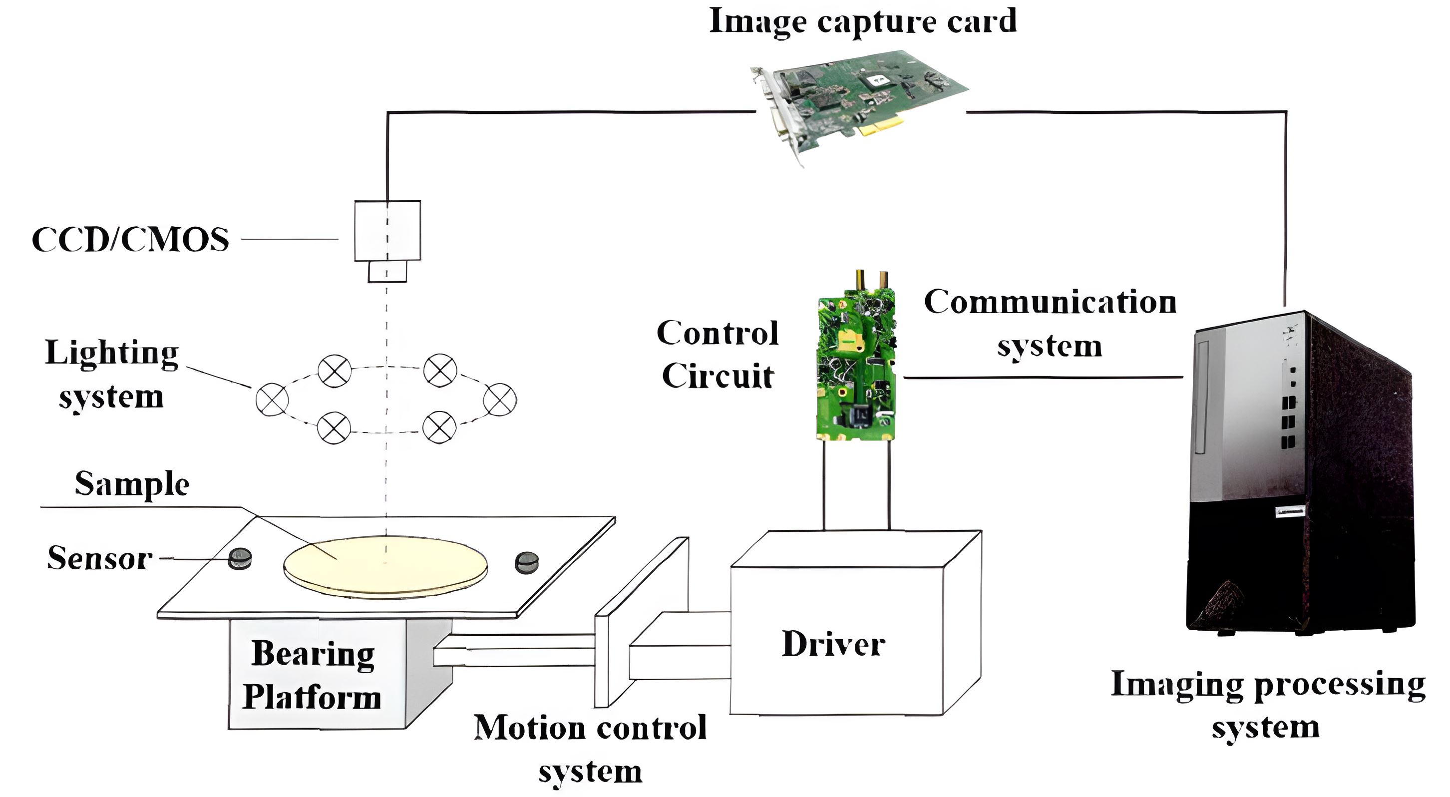
There are currently two main methods of defect inspection in the semiconductor industry: Automatic Optic Inspection (AOI) and Scanning Electron Microscope (SEM). The AOI system is based on optical principles. The main method is to illuminate the measured target by designing an illumination system (divided into bright field, dark field, transmission field and other imaging methods), using the imaging system to image the measured object, and through the image sensor (CMOS/CCD) is converted into digital image signals and then the upper computer system performs image analysis to achieve defect inspection. The SEM system collects extremely high energy and extremely narrow electron beams to bombard the surface of the sample to be tested, and collects particles generated by the interaction between the scanning beam and the material point by point to obtain various physical information.
Typical schematic diagram of AOI system (Photo source: Internet)
Comparing the two methods, the advantages of the AOI system are: 1) It is fast, and it takes very little time to capture an image using an area array image sensor. 2) Low cost. Cameras, light sources, and lenses can be freely combined, effectively reducing equipment costs. 3) The field of view is large and the imaging range is wide. Choosing the appropriate lens can achieve full-scale inspection of the wafer (Full Scale Scan), significantly improving the throughput of the equipment (Throughput). The disadvantages of AOI systems are that the imaging resolution is low and the characteristics of wafer defects are not obvious. The advantages of the SEM system are high resolution and high accuracy. However, because it is inspected point by point, it is extremely slow and expensive, and cannot meet the requirements of mass production in the semiconductor industry.
Today, with the developments of artificial intelligence (AI) technology and big data, AOI system is more than just an inspection equipment. They can classify and count a large number of wafer defects to discover the causes of defects. In process improvement and production yield improvement, it is also gradually playing a more and more important role. Therefore, it can be expected that automatic optical inspection technology will play an increasingly important role in semiconductor inspection in the future.
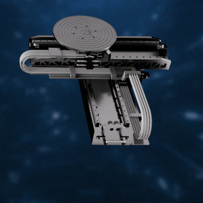
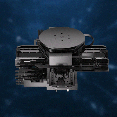
For semiconductor AOI systems, YiNGUAN Semiconductor can provide platform solutions that are compatible with 6/8/12-inch wafers and are compatible with Frame solutions. At the same time, in order to cope with different EFEMs, we also provide lift pin options. To improve measurement accuracy and throughput, you can choose our autofocus solution. YiNGUAN Semiconductor has an after-sales team covering major cities across the country to provide you with a full range of technical support.