(Photo source: Internet)
In semiconductor manufacturing, the thickness of the wafer film has an important impact on the performance and quality of the device. The thickness of the wafer film determines many important physical and chemical properties, and has a direct impact on its optical properties of refraction, reflection and transmission, which can lead to significant quantum size effects, thus changing the electronic, optical and magnetic properties of the material. Accurately measuring and controlling thickness of wafer films plays an important role in optimizing device performance, improving production efficiency, and ensuring device reliability.
Film thickness metrology can be divided into two basic types based on film materials, namely opaque films (metallic) and transparent films. The method of measuring the thickness of opaque films is usually by measuring the sheet resistance and obtaining the film thickness through its resistance and cross-sectional area. The equipment used is generally a four-probe station. The four probes are placed at equal distances and the outermost two probes are measured. The probe applies a current, thereby measuring its potential difference to calculate the sheet resistance of the film being measured. Transparent films, on the other hand, are usually based on ellipsometry technology, which analyzes polarization changes in the spectral range, and various film layers provide high-precision film measurements. Since film stress, refractive index and other physical properties also require elliptical polarization and interference technology to be measured, current mainstream film thickness metrology equipment integrates stress measurement, refractive index measurement and other functions.
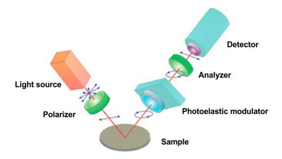
Figure 1. Schematic diagram of elliptical polarization measurement principle (Photo source: Internet)
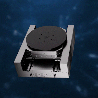
For wafer film thickness metrology equipment, YiNGUAN Semiconductor can provide an extremely compact motion system solution to supports flexibly and effectively customers' integrated or independent film thickness metrology solutions. The motion system adopts an innovative dual-axis coupling design concept and unique large-stroke maglev gravity compensation technology, which reduces the load on the vertical motor and greatly improves the vertical motion performance and lifespan. In addition, we also provide matched drivers, controllers and vibration isolation system to achieve measurement capabilities with high throughput. YiNGUAN Semiconductor has an after-sales team covering major cities across the country to provide you with a full range of technical support.